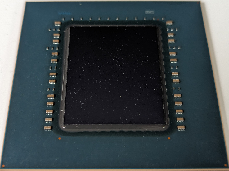
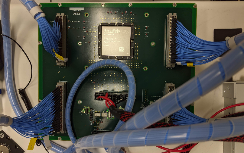
NORTHPOLE (12nm in 2021)
Created at IBM, NorthPole is a high-performance, high-efficiency neural network inference accelerator. It uses local memory within a parallel, distributed array of 256 cores, linked by NoCs. Fabbed in a 12nm finFET process, the chip has 224 MB of SRAM and uses 22 billion transistors. It represents the most efficient chip to date for several inference tasks (such as Resnet-50 classification and Yolov4 detection).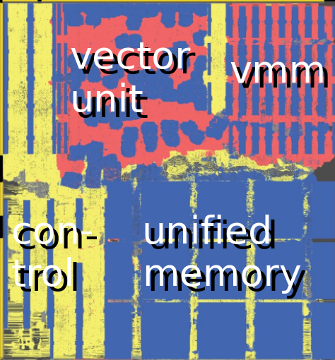
TRUENORTH (28nm in 2013)
Created at IBM, TrueNorth is the largest neuromorphic chip fabricated with one million configurable neurons and 256 million programmable synapse spread across 4,096 digital neurosynaptic cores, which only consume ~70mW. It has over 400 Mbits of embedded SRAM and uses 5.4 billion transistors. 16 TrueNorth Chips assembled into a 4x4 mesh form the largest neuromorphic system constructed with 16 million neurons and 4 billion synapses.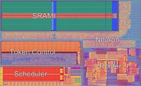
GOLDEN GATE (45nm in 2010)
Also from IBM, Golden Gate (along with its sister chip, San Francisco) was the first neurosynaptic core. It included 256 digital neurons and 256k programmable synapses. It was the first neuromorphic chip with a spike accurate simulator, allowing applications to be developed while the chip was being designed and fabricated.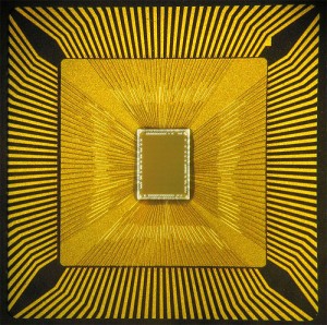
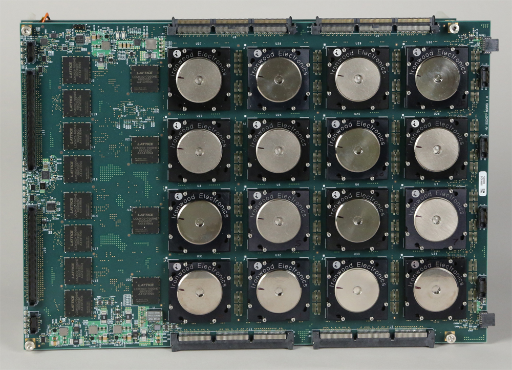
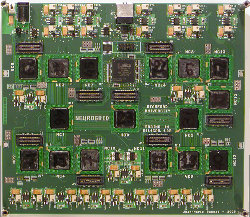
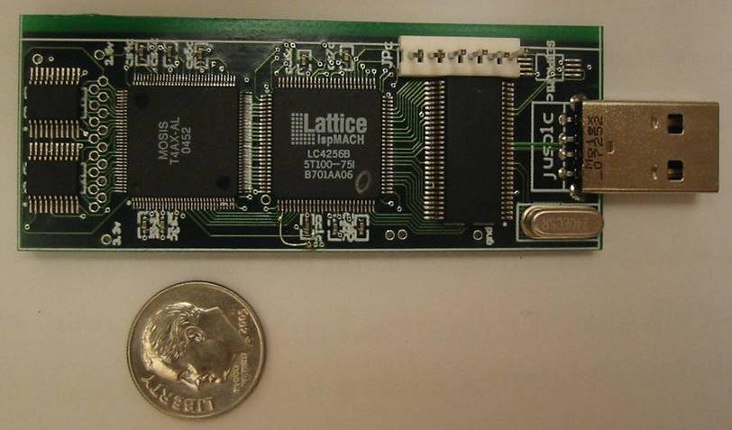
NEUROCORE & NEUROGRID (180nm in 2007)
Developed at Stanford, the Neurocore Chip was the first chip with 65k neuron, each with two compartments and a set of configurable silicon ion channels. Sixteen Neurocores are assembled on a board to create a million-neuron Neurogrid. Notice that the Neurocore test board (left) has clear epoxy, leaving the die visible.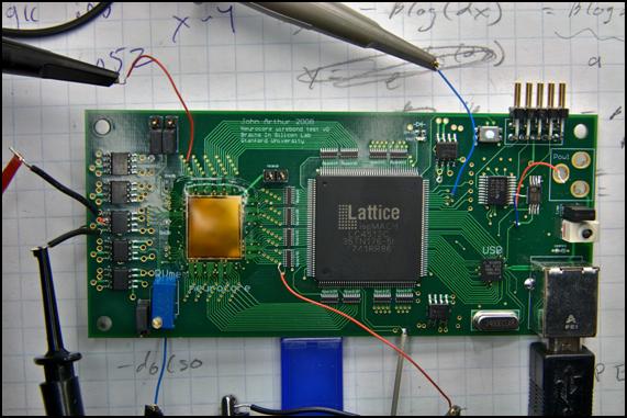
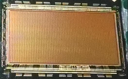
THESIS CHIP (250nm in 2005)
My Thesis Chip (at UPenn) has gone by many names but from my perspective its most important contribution is that it helped me graduate. It was later the basis for a class at Stanford. It provided the substrate for studies in single neuron dynamics, neuronal network synchrony, and the role of spike timing-dependent plasticity in storing patterns and compensating for mismatch among neurons.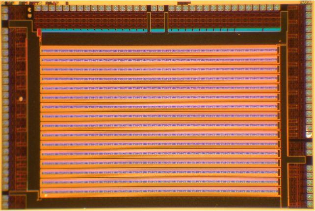
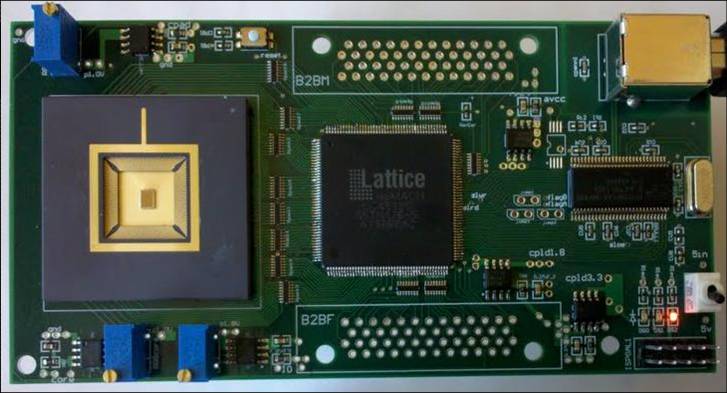
DENDRITE CHIP (250nm in 2003)
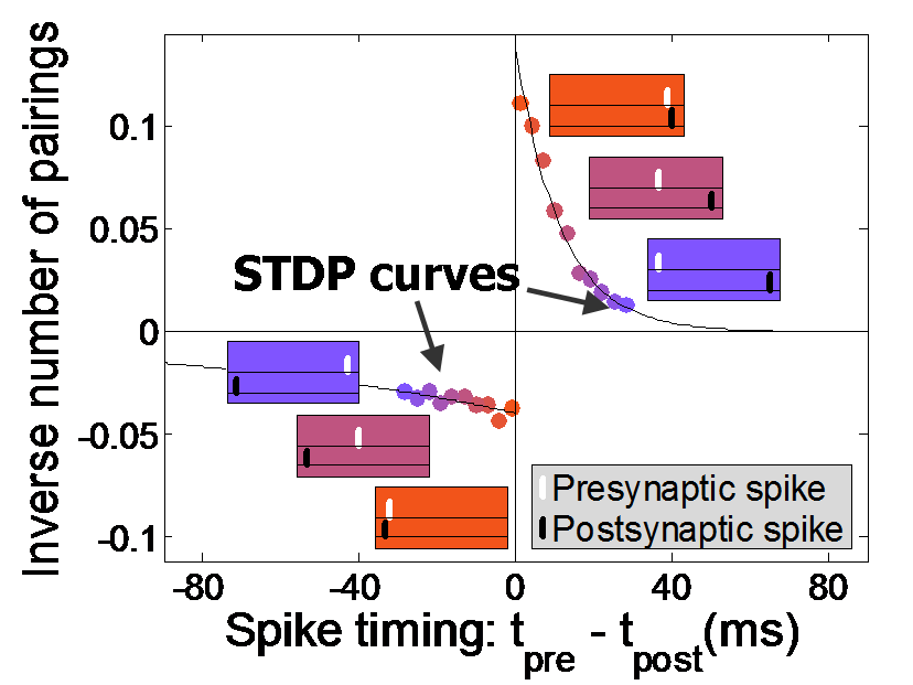
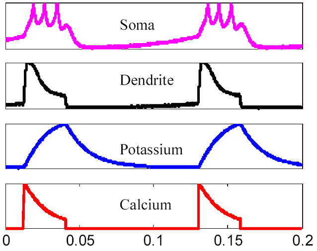
The Dendrite Chip was the first chip that I designed myself. It includes the first log-domain conductance-based spiking neuron circuit, possibly the first multi-compartment silicon neuron (45 dendrite compartments plus a soma), and an early form of spike timing-dependent synaptic plasticity.
More
|
|
John Arthur |
